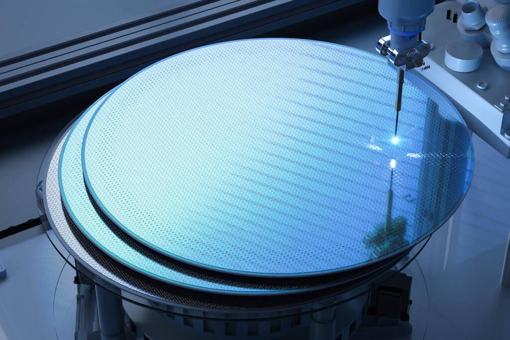
半导体材料图片

半导体材料新闻每周精选
图片尺寸952x770
8月份半导体材料的3只科技龙头股
图片尺寸611x377
我国碳基半导体制备材料取得关键性突破
图片尺寸740x462
国内芯片行业迎来福音,半导体材料冲破世界前六打破日本市场垄断
图片尺寸640x418
一文看懂半导体材料
图片尺寸760x507
立方砷化硼是最好的半导体材料
图片尺寸777x518
semi:台湾蝉联全球最大半导体材料市场
图片尺寸600x411
半导体光电材料是什么?
图片尺寸640x441
第三代半导体材料-碳化硅介绍
图片尺寸974x544
年度业绩预告盘点 半导体材料企业的喜与愁
图片尺寸1000x750
> tag信息列表 > 有机半导体材料
图片尺寸557x300
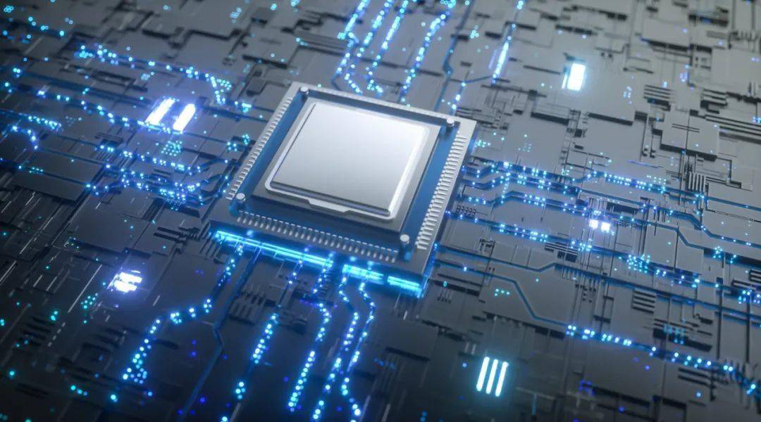
第三代半导体图片
图片尺寸200x300
semi : 2022年半导体材料市场规模有望达到698亿美元,创下新高 - 艾邦
图片尺寸2560x1440
作为半导体芯片制造基石2022年半导体材料市场创698亿美
图片尺寸1000x667
投资数十亿日元三菱化学计划在日本国内新建半导体材料工厂附半导体
图片尺寸760x505
《2020-2026年中国半导体硅材料行业竞争格局分析及投资潜力研究报告
图片尺寸680x461
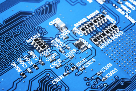
科技半导体图片
图片尺寸450x300
后摩尔时代碳基半导体从材料突围
图片尺寸1080x600
重磅宣布上海将推动非硅基半导体材料技术研究和布局
图片尺寸640x350
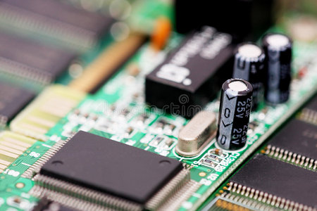
半导体元件图片
图片尺寸450x300