欧姆接触能带图

肖特基势垒与欧姆接触
图片尺寸2030x854
资料 p型器件在平带,积累,耗尽,反 型情况下的能带图和对应的电荷块图
图片尺寸1080x810
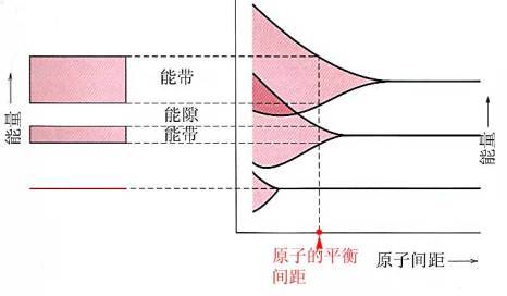
从能带论的角度解释导体,半导体和绝缘体的导电能力存在差异的原因.
图片尺寸614x474
能带理论--能带结构中部分概念的理解小结
图片尺寸893x513
mos电容c-v特性ppt 无偏压下mos电容结构的能带图 ws wm 的接触电势
图片尺寸1080x810
能带
图片尺寸200x207
mos二极管中三个分离系统的能带图
图片尺寸1080x810
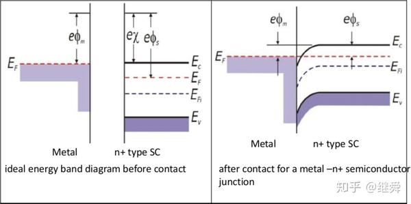
画出n型和p型硅衬底上理想的金属-半导体接触(理想金属-半导体接触的
图片尺寸479x258
半导体器件物理ppt
图片尺寸1080x810
能带 (其他物理学相关)
图片尺寸466x272
肖特基势垒与欧姆接触
图片尺寸1990x700
mos 能带图
图片尺寸707x675
通过激光激发和压电电荷的耦合调制的m-s肖特基接触的能带示意图(a)
图片尺寸600x1042
肖特基势垒与欧姆接触
图片尺寸600x299
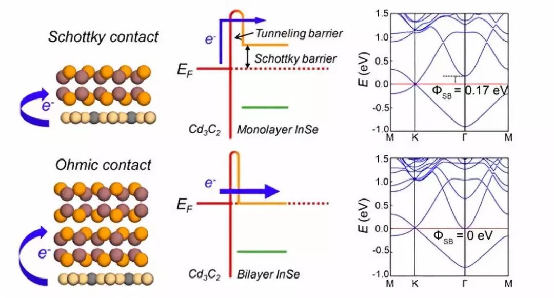
必看!肖特基接触到欧姆接触的转变
图片尺寸1080x581
关于能带ek图的问题
图片尺寸800x591
欧姆接触
图片尺寸220x134
画出n型和p型硅衬底上理想的金属-半导体接触(理想金属-半导体接触的
图片尺寸469x264
接触的含义:金属-半导体界面无界面态,不考虑镜像电荷的作用)的能带图
图片尺寸757x427
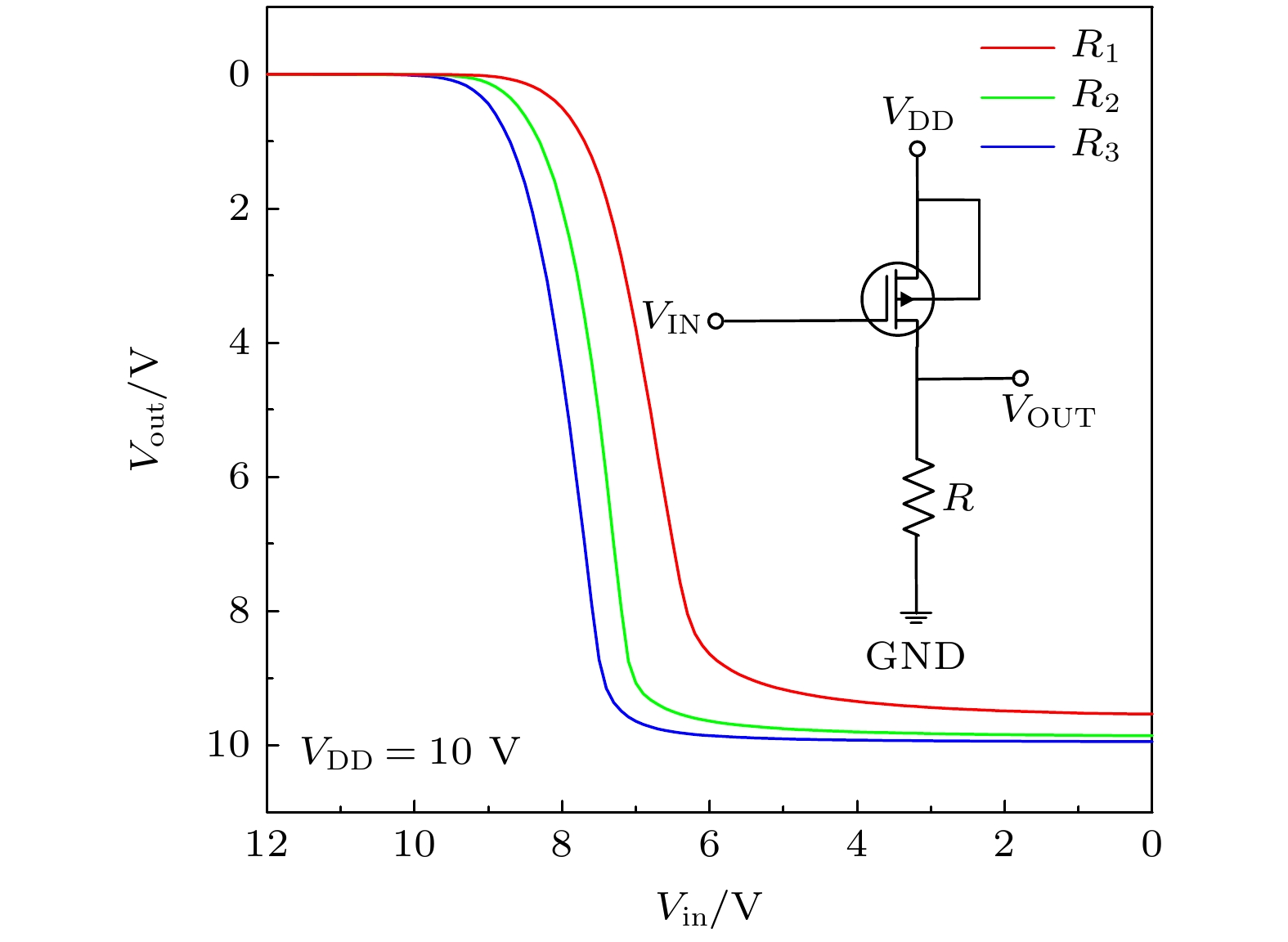
测试结果如图2所示, 三个电阻都表现出非常好的欧姆接触特性(图2(a))
图片尺寸1575x1152