芯片设计流程

数字ic设计流程总结_数字ic芯片设计流程图-csdn博客
图片尺寸1111x1292
芯片流程
图片尺寸1329x734
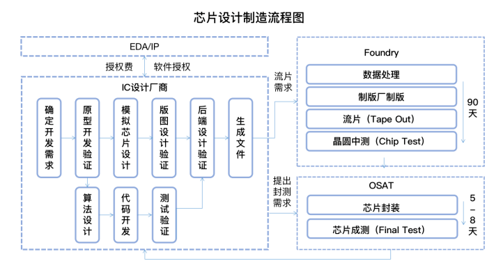
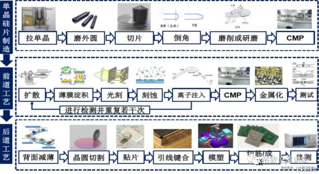
芯片制造流程参考图
图片尺寸1030x974
芯片行业的秘密_设计的_集成电路_工具
图片尺寸709x398
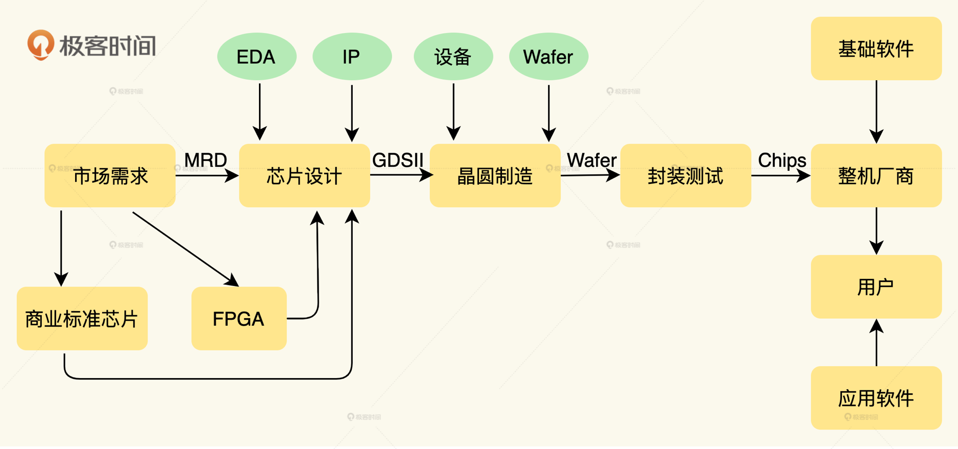
03 | 芯片设计:一颗芯片到底是如何诞生的(上)
图片尺寸1876x879
模拟芯片设计流程和数字ic区别
图片尺寸640x643
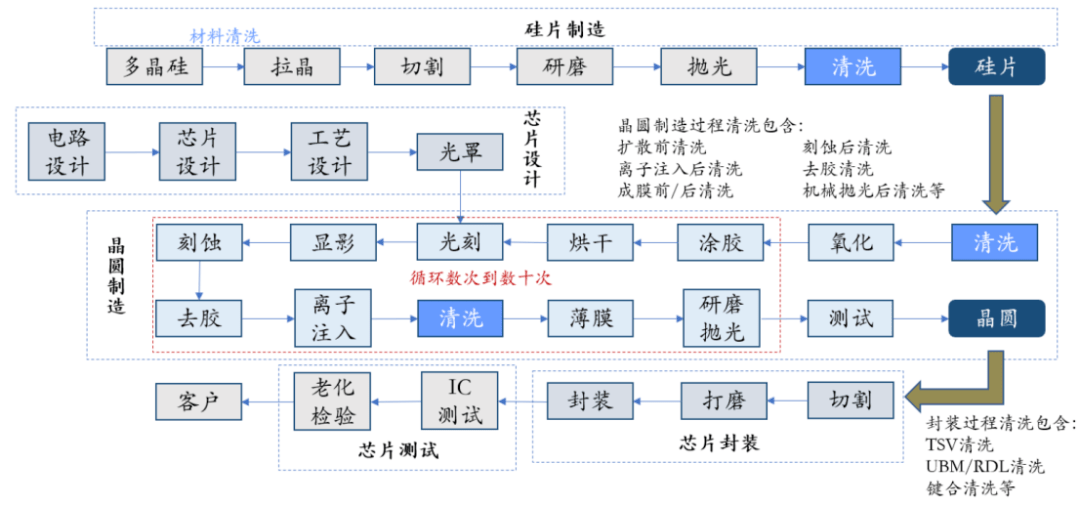
芯片制造,洗洗更健康
图片尺寸1080x506
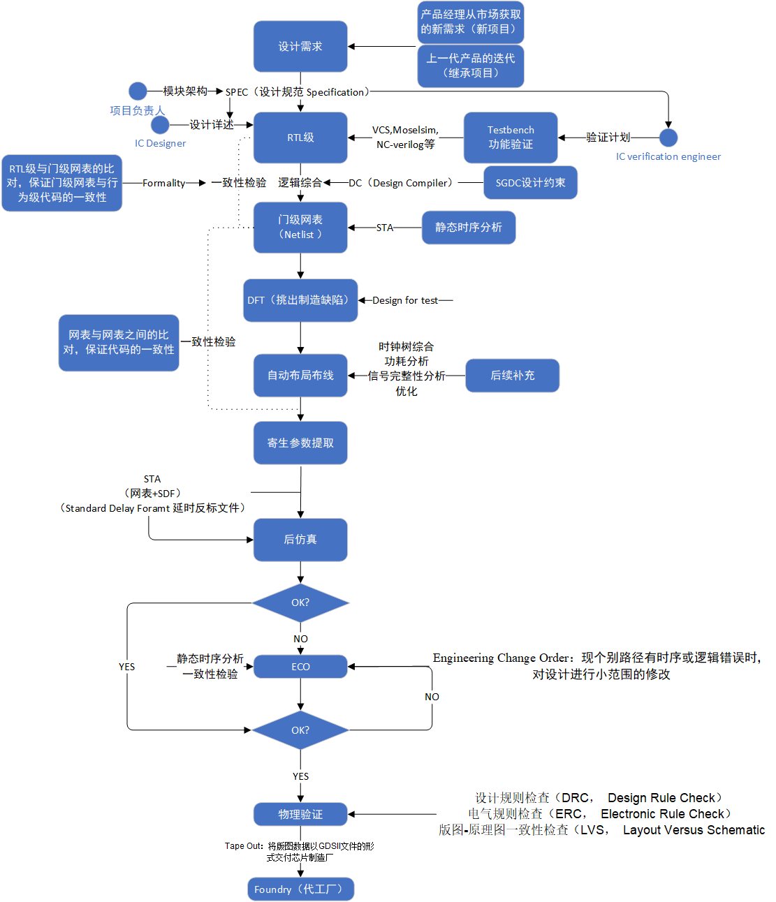
二.数字ic设计流程,借鉴这个图
图片尺寸781x494
集成电路eda设计概述
图片尺寸1200x900
一文揭秘芯片之母eda产业国产路在何方?
图片尺寸1175x646
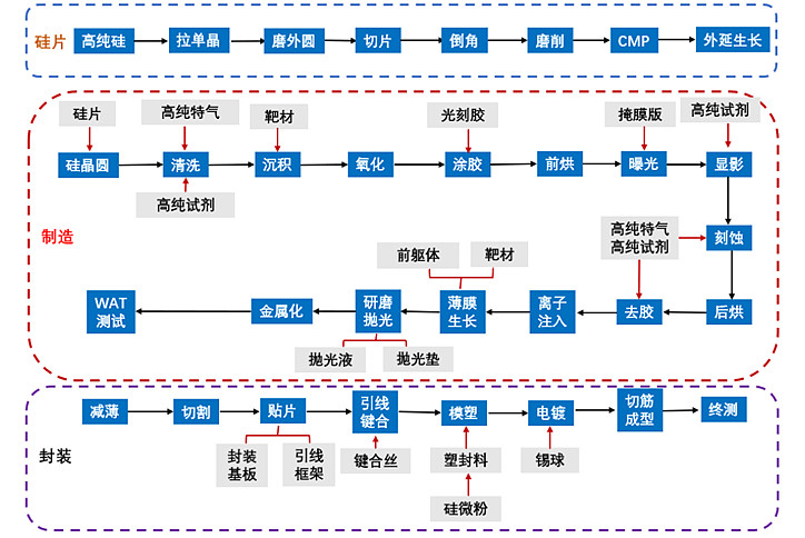
集成电路芯片制造工艺流程示意图真正去看集成电路的制造工艺,如果从
图片尺寸1080x589
芯片设计流程
图片尺寸740x678
一文了解芯片的分类,设计流程和相关职位
图片尺寸640x471
芯片设计流程
图片尺寸720x404
单片机应用系统设计过程流程图
图片尺寸3432x3160
一款智能驾驶ai芯片的设计与制造流程
图片尺寸653x665
工程科技 信息与通信 模拟集成电路设计ppt 模拟集成电路设计流程
图片尺寸1080x810
【转载】数字ic设计流程及开发工具
图片尺寸1498x663
半导体芯片工艺流程及材料应用在芯片制造,封测过程中使用到的半导体
图片尺寸724x484
芯片设计又可以分为两部分,芯片前端设计和芯片后端设计,整体流程如下
图片尺寸1082x558