die bonding

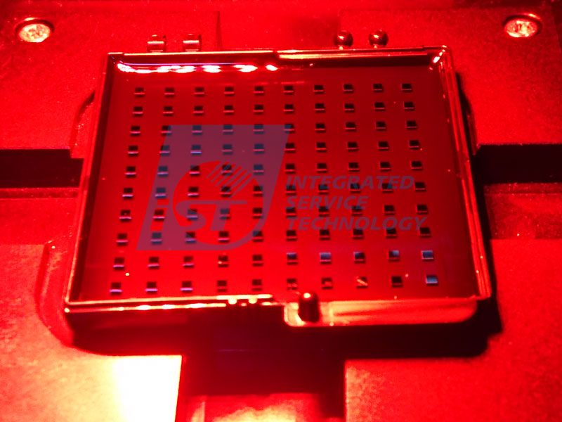
奇石乐die or wire bonding(绑定)产品测试
图片尺寸550x550
die bond process introduction
图片尺寸1080x810
diebonding制程培训
图片尺寸1077x808
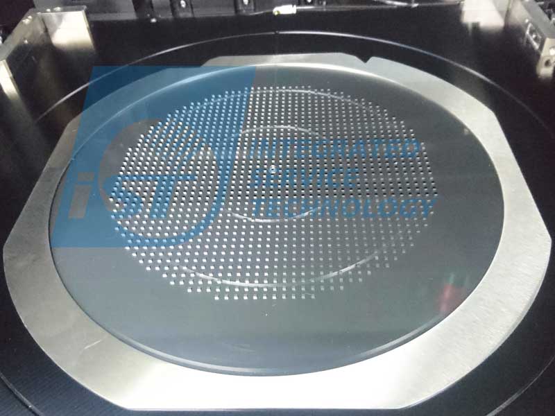
该工艺将晶圆分成单个的芯片,用于随后的芯片接合(die bonding),引线
图片尺寸800x399
cob die bonding
图片尺寸680x440
硅光相关概念waferdiechip以及bonding
图片尺寸720x436
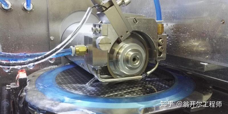
高精度多功能粘晶服务diebonding
图片尺寸800x600
diebonding制程培训
图片尺寸1077x808
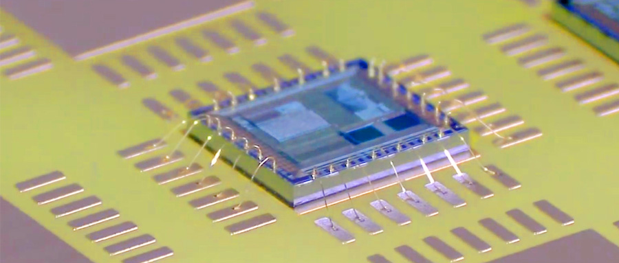
将芯片固定于封装基板上的工艺芯片键合diebonding
图片尺寸1000x404
ad832u automatic eutectic die bonding system
图片尺寸3111x2829
high-throughput multiple dies-to-wafer bonding technology and
图片尺寸1158x610
latest product automatic die bonding system (12" wafer handling
图片尺寸4928x3264
chemicalbondingii超详细重点总结
图片尺寸1080x1439
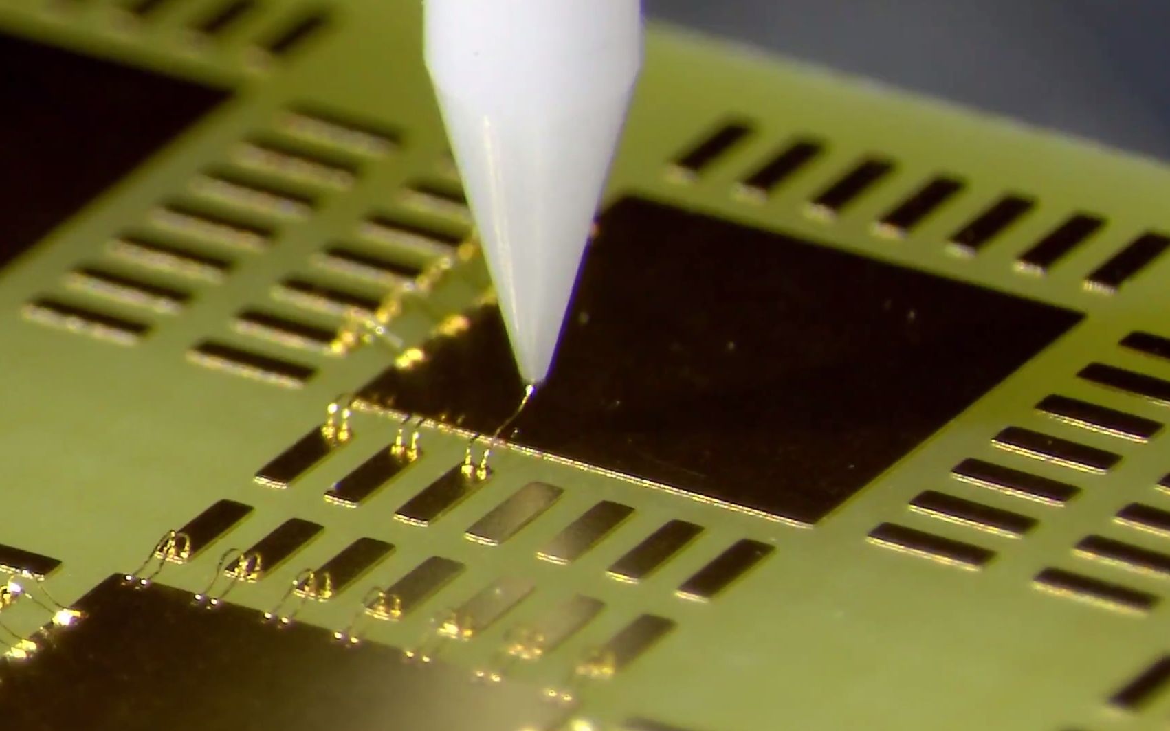
wire bond,die bond 是什么意思,有什么区别?
图片尺寸900x383
科普芯片行业术语汇总
图片尺寸640x373
德国的三种芯片键合工艺wedgebondingballbondingbumpbonding
图片尺寸1702x1064
将芯片固定于封装基板上的工艺芯片键合diebonding
图片尺寸1000x331
高精度多功能粘晶服务diebonding
图片尺寸800x600
high-throughput multiple dies-to-wafer bonding technology and
图片尺寸992x481
沛顿科技(深圳)有限公司
图片尺寸509x975