gate oxide

creation of multiple gate oxide with high thickness ratio in
图片尺寸2320x3408
gate formation (i) sac oxide remove gate1 oxide dep
图片尺寸1080x810
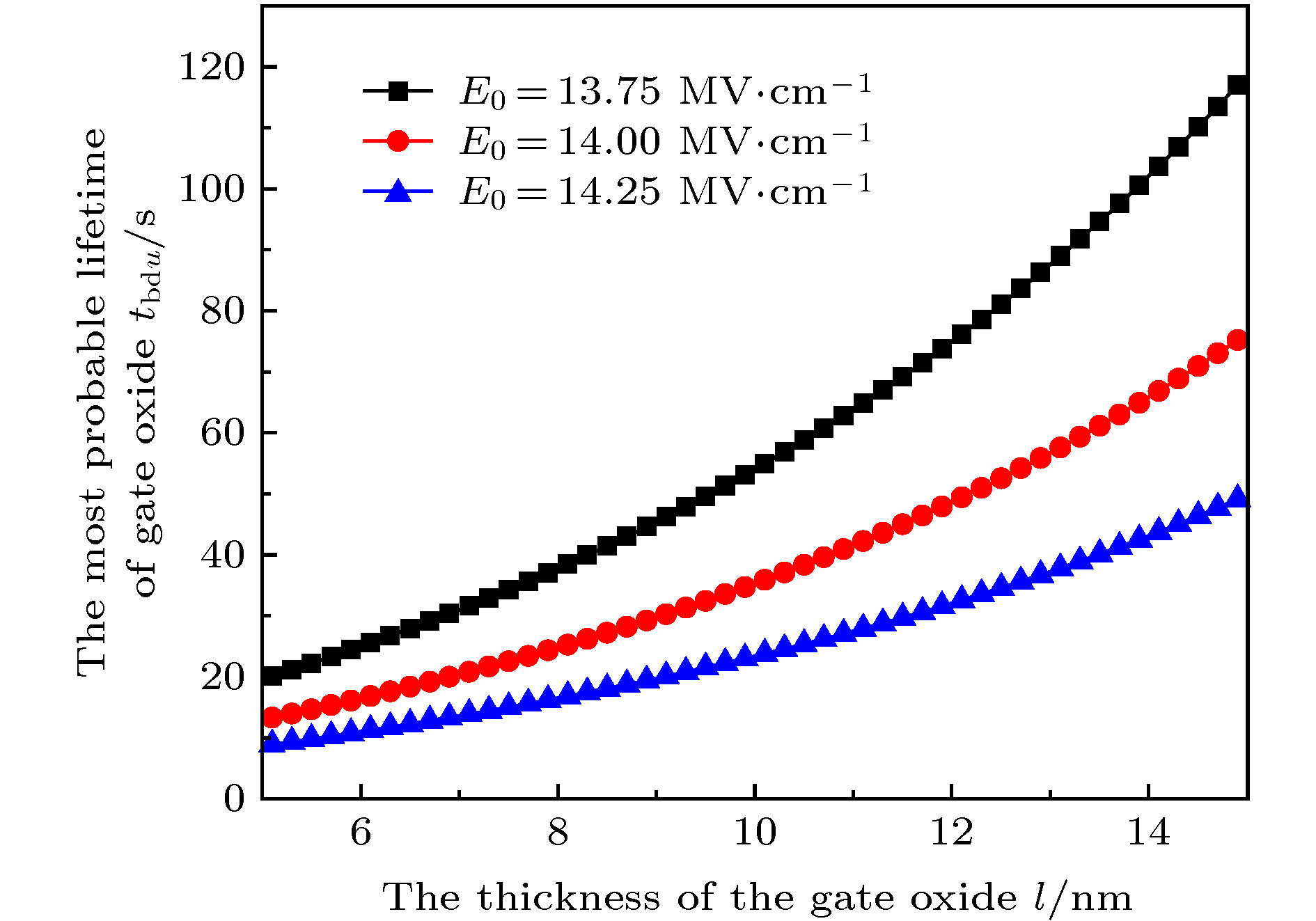
statistical theoretical analysis method of tddb of gate oxide
图片尺寸1890x2698
可靠性系列gateoxidedegradation
图片尺寸1440x624
03 gate oxide degradation
图片尺寸722x303
dual gate oxide structure in semiconductor device and method
图片尺寸1725x2441
statistical theoretical analysis method of tddb of gate oxide
图片尺寸1890x1323
gate oxide short defect model in finfets
图片尺寸266x312
system and method for testing gate oxide of an amplifier
图片尺寸1658x2626
03 gate oxide degradation
图片尺寸566x458
method of fabricating a dual gate oxide
图片尺寸1521x642
trench semiconductor device having gate oxide layer with
图片尺寸2053x3170
high-density plasma multilayer gate oxide
图片尺寸2053x2690
method of simulation for gate oxide integrity check on an entire
图片尺寸2701x4108
thermal dual gate oxide device integration
图片尺寸2092x2581
method of forming a low voltage gate oxide layer and tunnel
图片尺寸2035x2092
method of forming nitrogen implanted ultrathin gate oxide for
图片尺寸2437x3789
method for determining transistor gate oxide thickness
图片尺寸2566x2608
use of oxide surface to facilitate gate break on a carrier
图片尺寸2342x2569
专利us6753229 - multiple-thickness gate oxide formed by oxygen
图片尺寸2290x3747