plasma etch

plasma_etch
图片尺寸1188x918
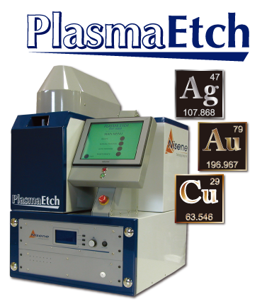
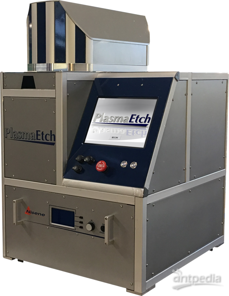
等离子芯片开封机plasmaetch
图片尺寸370x429
nisene等离子芯片开封机plasmaetch
图片尺寸600x774
【etch】plasma etch process - an introduction
图片尺寸900x675
【etch】plasma etch process - an introduction
图片尺寸900x675
【etch】plasma etch process - an introduction
图片尺寸900x675
plasma etch resistant coating and process
图片尺寸1581x2536
海外直订plasma etching: fundamentals and applications 等离子体
图片尺寸800x800
plasma etch pe-50 bench top system
图片尺寸500x500
【etch】plasma etch process - an introduction
图片尺寸900x675
mask etch plasma reactor with variable process gas distribution
图片尺寸2084x2745
plasma etch reactor and method for emerging films
图片尺寸2694x3463
plasma dielectric etch process including ex-situ backside
图片尺寸1665x2470
mask etch plasma reactor with variable process gas distribution
图片尺寸2250x2769
dielectric plasma etch with deep uv resist and power modulation
图片尺寸2248x734
plasma etch techniques for fabricating silicon structures from a
图片尺寸2716x3947
【etch】plasma etch process - an introduction
图片尺寸900x675
【etch】plasma etch process - an introduction
图片尺寸900x675
【etch】plasma etch process - an introduction
图片尺寸900x675
plasma etch techniques for fabricating silicon structures from a
图片尺寸2628x3658