qfn封装工艺流程

封装浅析:封装形式演进带来工艺流程变革
图片尺寸725x434
ic封装流程简介
图片尺寸664x461
第27页 (共33页,当前第27页) 你可能喜欢 芯片封装测试 ic封装工艺 ic
图片尺寸1082x812
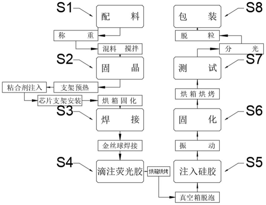
整个led封装工艺流程都是按照如图2所示的流程制作的
图片尺寸713x516
ic封装工艺流程图传统封装
图片尺寸1490x694
二三极管封装工艺
图片尺寸560x348
简单了解芯片封装技术
图片尺寸1280x426
一种圆片级led芯片的封装方法与流程
图片尺寸870x670
电子封装技术 封装工艺流程
图片尺寸1080x810
典型半导体封装工艺流程后道
图片尺寸779x599
封装流程介绍ppt
图片尺寸1080x810
led封装制作及成品组装流程图
图片尺寸540x911
塑料封装的前段工艺流程示意图
图片尺寸500x339
或者与bga,lga,csp(chip level package)封装相比,qfn封装的流程都并
图片尺寸562x258
ic封装流程ppt
图片尺寸1080x810
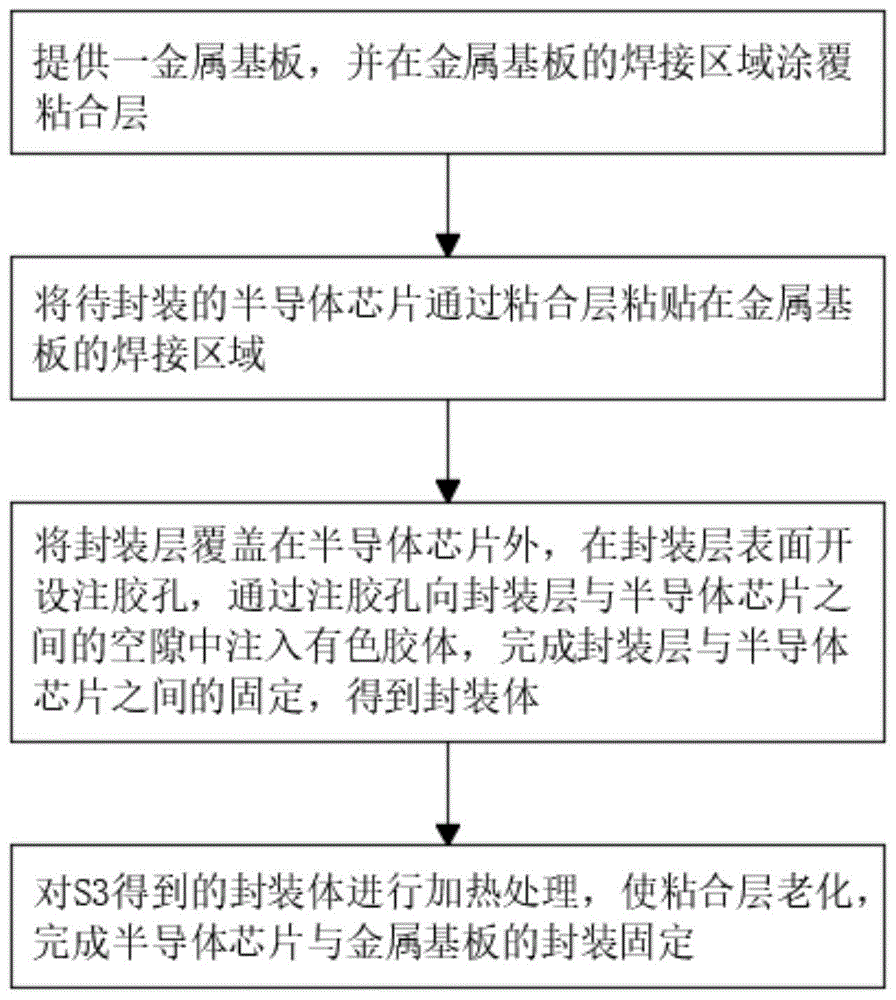
半导体芯片的封装方法与流程
图片尺寸812x1000
传统封装工艺流程
图片尺寸1080x810
陶瓷材料在芯片管壳中的封装工艺流程-应用于激光管壳封装制造
图片尺寸640x326
一种半导体芯片的封装方法与流程
图片尺寸896x1000
ic封装工艺流程
图片尺寸1080x810